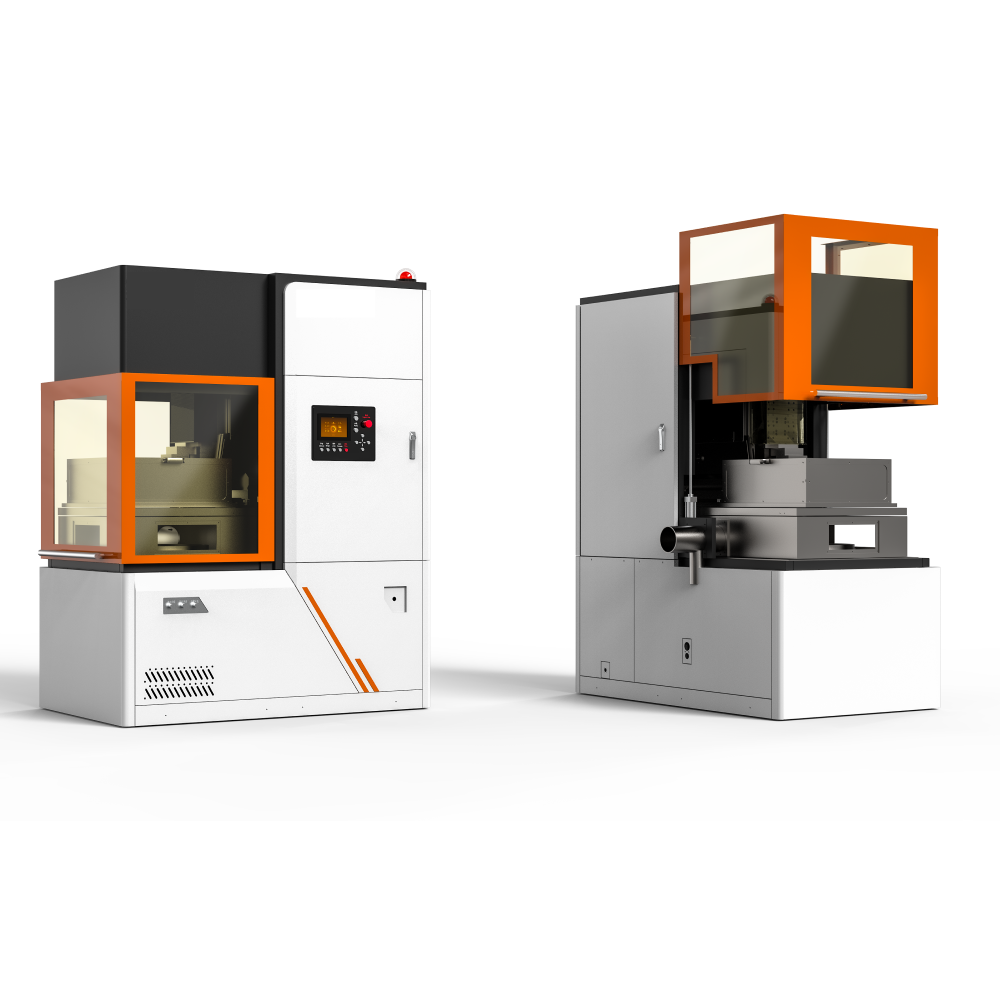
1.Equipment for scribing and splitting semiconductor substrates such as GaAs and Inp.
2.Can be used for R&D and mass production.
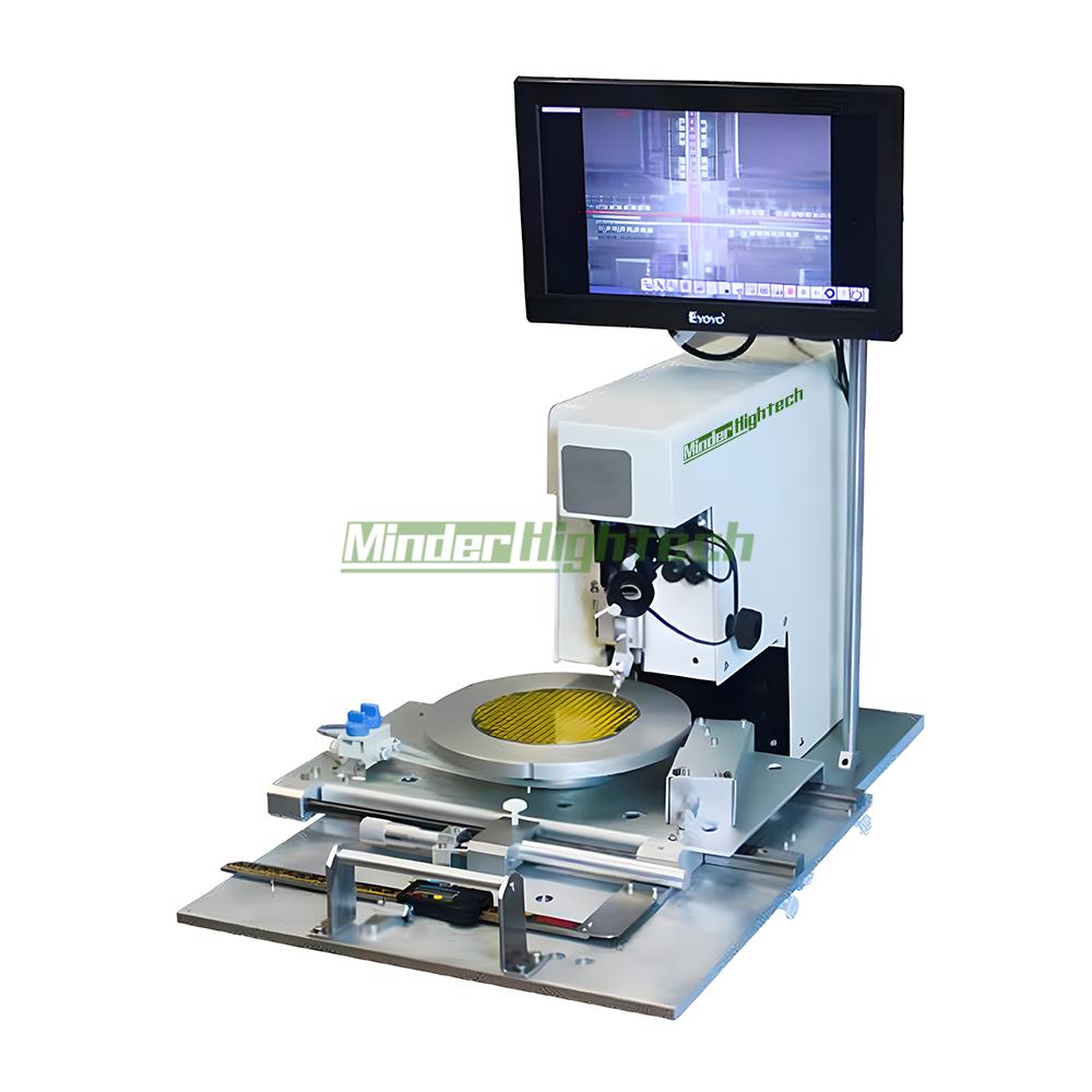
Features
1. The maximum wafer size that can be scratched is 8 inches.
2. The scratch width is ≤ 10μm.
3. The resolution is 1μm.
联系人:胡顺语
手机:0086-15813334038
电话:020-84789496
邮箱:md@minder-hightech.com
地址: 广州市番禺区大龙街市新路新水坑段43号813