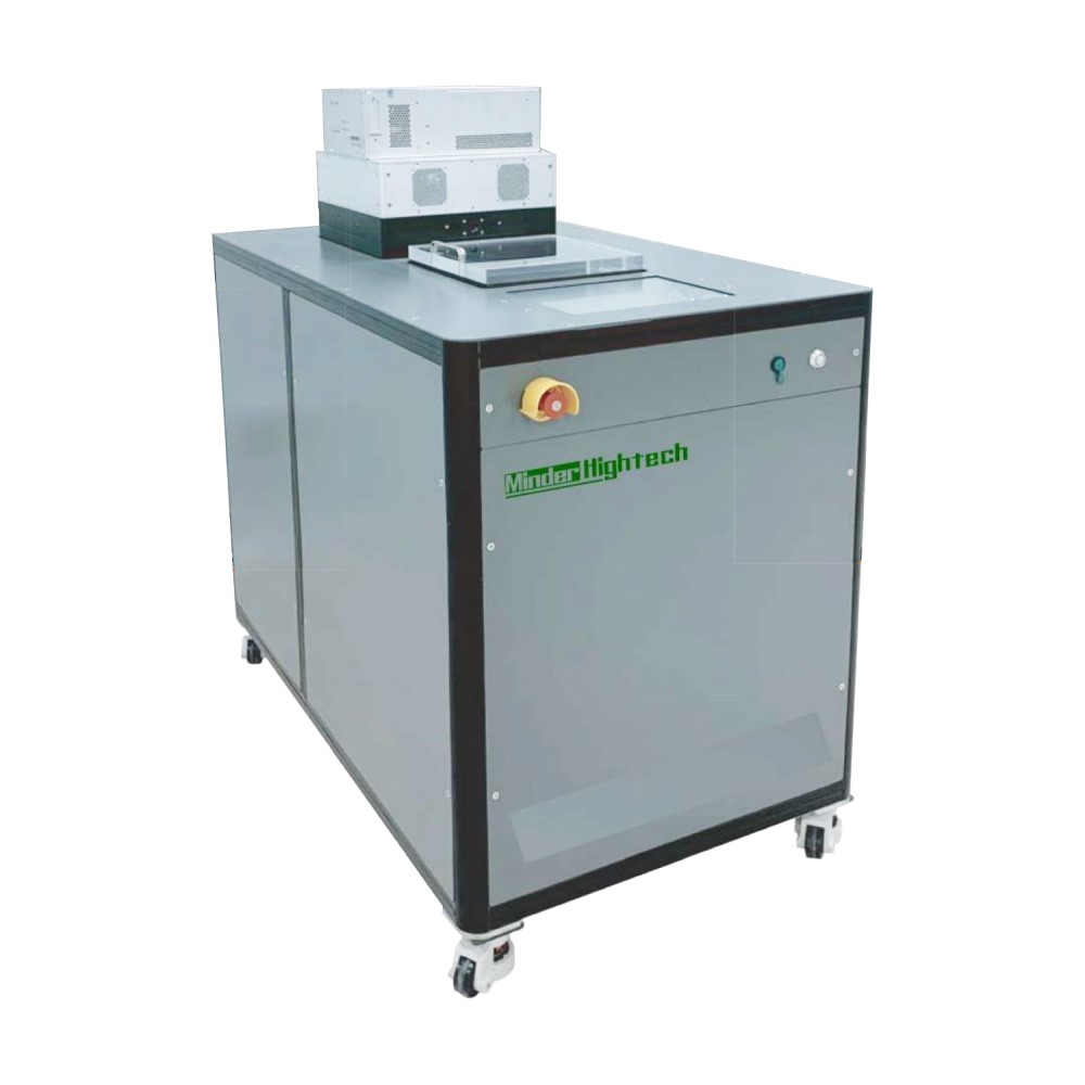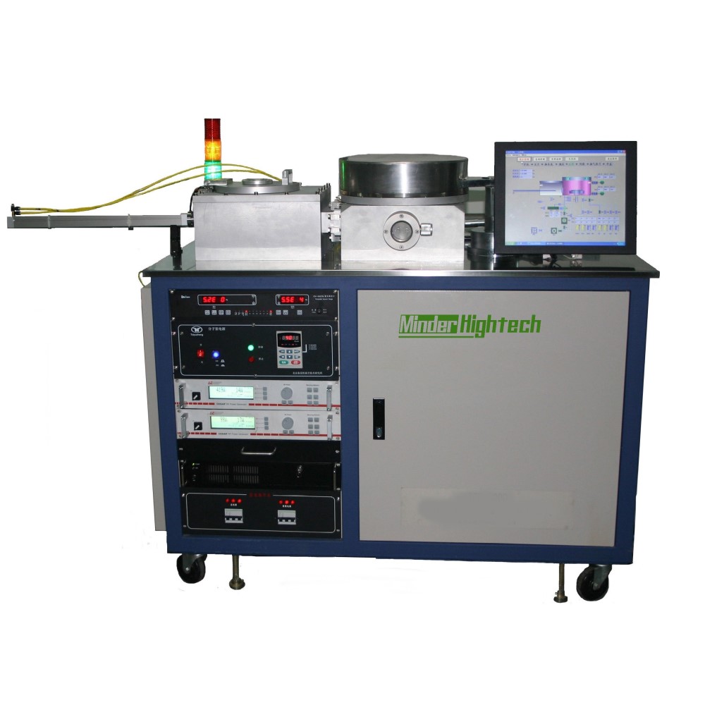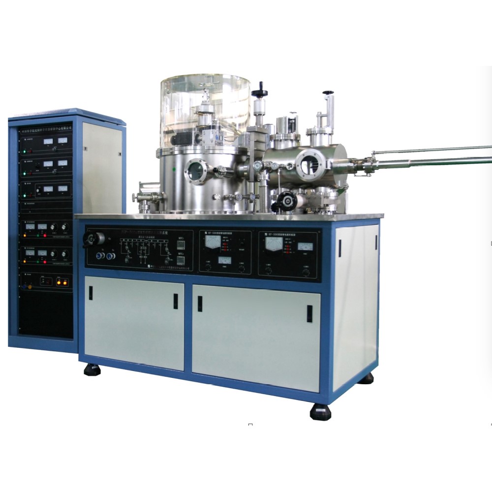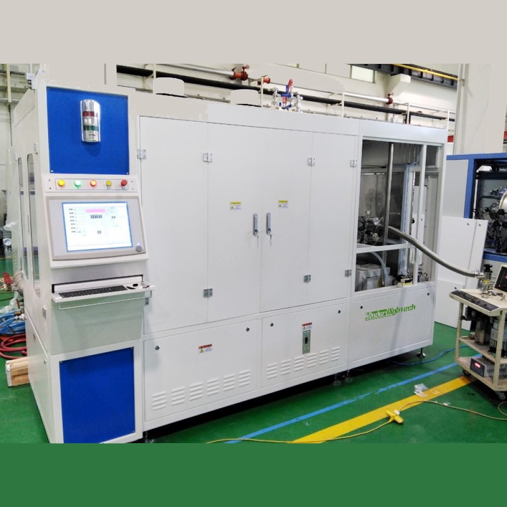


Reactive ion etching system
Project configuration and machine structure diagram
|
Item |
MD150-RIE |
MD200-RIE |
MD200C-RIE |
|
Product size |
≤6 inches |
≤8 inches |
≤8 inches |
|
RF power source |
0-300W/500W/1000W Adjustable,automatic matching |
||
|
Molecular pump |
-/620(L/s)/1300(L/s)/Custom |
Antiseptic620(L/s)/1300(L/s)/Custom |
|
|
Foreline pump |
Mechanical pump/dry pump |
Dry pump |
|
|
Process pressure |
Uncontrolled pressure/0-1Torr controlled pressure |
||
|
Gas type |
H/CH4/O2/N2/Ar/SF6/CF4/ CHF3/C4F8/NF3/Custom (Up to 9 channels, no corrosive & toxic gas) |
H2/CH4/O2/N2/Ar/F6/CF4/ CHF3/C4F8/NF3/Cl2/BCl3/HBr(Up to 9 channels) |
|
|
Gas range |
0~5sccm/50sccm/100sccm/200sccm/300sccm/500sccm/custom |
||
|
LoadLock |
Yes/No |
Yes |
|
|
Sample tem control |
10°C~Room tem/-30°C~100°C/Custom |
-30°C~100°C /Custom |
|
|
Back helium cooling |
Yes/No |
Yes |
|
|
Process cavity lining |
Yes/No |
Yes |
|
|
Cavity wall tem control |
No/Roomtem~60/120°C |
Room tem-60/120°C |
|
|
Control System |
Auto/custom |
||
|
Etching material |
Silicon-based:Si/SiO2/SiNx··· IV-IV: SiC Magnetic materials/alloy materials Metallic material: Ni/Cr/Al/Au..... Organic material: PR/PMMA/HDMS/Organic film...... |
Silicon-based: Si/SiO2/SiNx...... III-V(注3): InP/GaAs/GaN...... IV-IV: SiC II-VI (注3): CdTe...... Magnetic materials/alloy materials Metallic material: Ni/Cr/A1/Au...... Organic material: PR/PMMA/HDMS /organic film... |
|
Process result
Silicon-based material etching
Silicon-based materials, nano-imprint patterns, array
patterns and lens pattern etching

InP normal temperature etching
Pattern etching of InP based devices used in optical communication, including waveguide structure, resonant cavity structure ridge structure etc

SiC material etching
Suitable for microwave devices, power devices, etc

Physical sputtering, etching Organic materiale tching
|
It is applied to the etching of difficult to etch materials such as some metals (such as Ni / Cr) and ceramics, and the patternede tching of materials is realized by physical bombardment. |
It is used for etching and removal of organic compounds such as photoresist (PR)/ PMMA / HDMS / polymer |

Cermet film material (Au/Ni/Cr/Al2O3)
Contact: Minder Hu
Phone: 0086-15813334038
Tel: 020-84789496
Email: md@minder-hightech.com
Add: 813,No.43,Xinshuikeng Section, Shixin Road, Dalong street,Panyu District,Guangzhou. Zip:511442