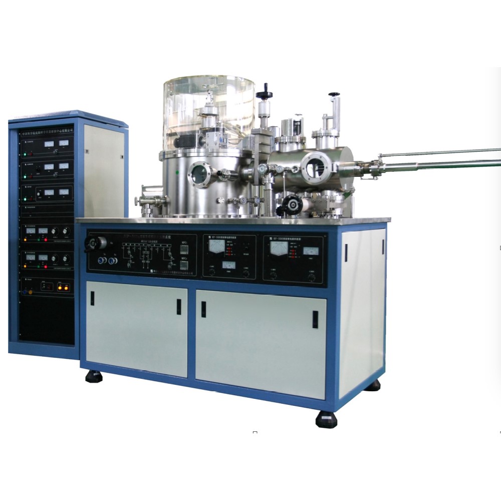


Inductive coupling plasma etching (icp) system
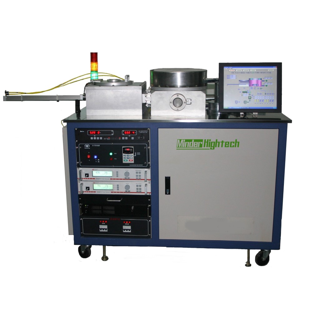
Project configuration and machine structure diagram
|
Item |
MD150S-ICP |
MD200S-ICP |
MD150CS-ICP |
MD200CS-ICP |
MD300C-ICP |
|
Product size |
≤6 inches |
≤8 inches |
≤6 inches |
≤8 inches |
Custom≥12inches |
|
SRF Power source |
0~1000W/2000W/3000W/5000WAdjustable,automatic matching\,13.56MHz/27MHz |
||||
|
BRF Power source |
0~300W/0~500W/0~1000WAdjustable, automatic matching,2MHz/13.56MHz |
||||
|
Molecular pump |
Non corrosive : 600 /1300 (L/s)/Custom |
Anti-corrosion:600 /1300 (L./s)/Custom |
600/1300(L/s) /Custom |
||
|
Foreline pump |
Mechanical pump / dry pump |
Anti corrosion dry pump |
Mechanical pump / dry pump |
||
|
Pre pumping pump |
Mechanical pump / dry pump |
Mechanical pump / dry pump |
|||
|
Process pressure |
Uncontrolled pressure/0-0.1/1/10Torr controlled pressure |
||||
|
Gas type |
H2/CH4/O2/N2/Ar/SF6/CF4/ CHF3/C4F8/NF3/NH3/C2F6/Custom (Up to 12 channels, no corrosive & toxic gas) |
H2/CH4/O2/N2/Ar/SF6/CF4/CHF3/ C4F8/NF3/NH3/C2F6/Cl2/BCl3/HBr/ Custom(Up to 12 channels) |
|||
|
Gas range |
0~5sccm/50sccm/100sccm/200sccm/300sccm/500sccm/1000sccm/Custom |
||||
|
LoadLock |
Yes/No |
Yes |
|||
|
Sample tem control |
10°C~Roomtem/ -30°C~150°C /Custom |
-30°C~200°C/Custom |
|||
|
Back helium cooling |
Yes/No |
Yes |
|||
|
Process cavity lining |
Yes/No |
Yes |
|||
|
Cavity wall tem control |
No/Room tem-60/120°C |
Room tem~60/120°C |
|||
|
Control System |
Auto/custom |
||||
|
Etching material |
Silicon-base: Si/SiO2/ SiNx/ SiC..... Organic materials:PR/Organic film...... |
Silicon-base: Si/SiO2/SiNx/SiC III-V: InP/GaAs/GaN...... IV-IV: SiC II-VI: CdTe...... Magnetic material / alloy material Metallic materials: Ni/Cr/Al/Cu/Au... Organic materials: PR/Organic film...... Silicon deep etching |
|||
Process result
Quartz / silicon / grating etching
Using BR mask to etch quartz or silicon materials, the grating array pattern has the thinnest line up to 300nm and the sidewall steepness of the pattern is close to > 89°, which can be applied to 3D display, micro optical devices, optoelectronic communication, etc

Compound / semiconductor etching
Accurate control of sample surface temperature can well control the etching morphology of GaN based, GaAs, InP and metal materials. lt is suitable for blue lED devices, lasers, optical communication and other applications.

Silicon-based material etching
it is suitable for etching silicon based materials such as Si, SiO2, and SiNx. lt can realize silicon line etching above 50nm and silicon deep hole etching below 100um

Contact: Minder Hu
Phone: 0086-15813334038
Tel: 020-84789496
Email: md@minder-hightech.com
Add: 813,No.43,Xinshuikeng Section, Shixin Road, Dalong street,Panyu District,Guangzhou. Zip:511442