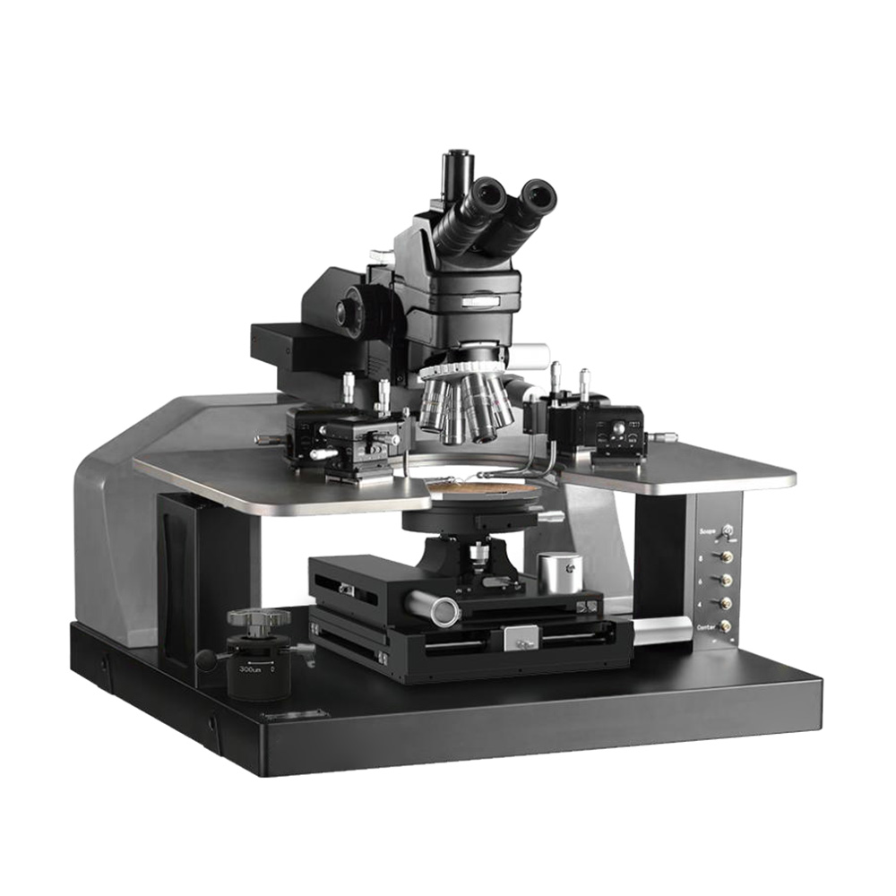
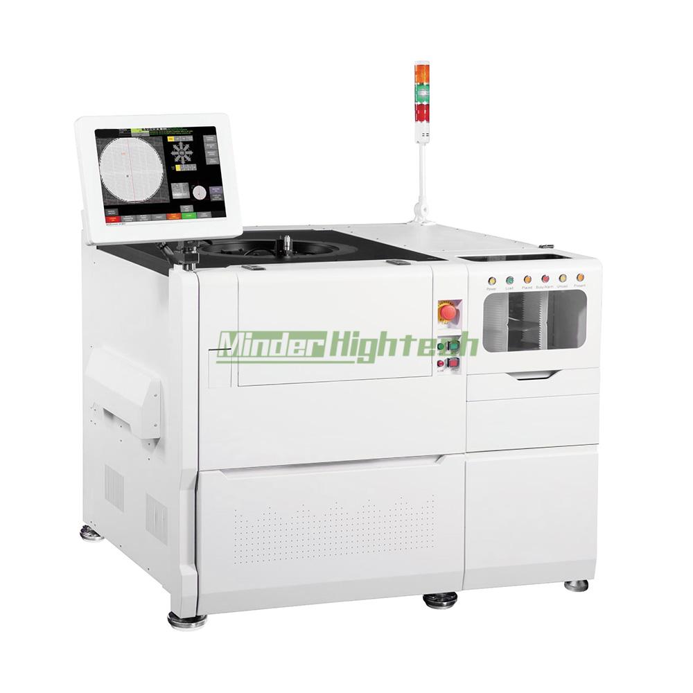
Product Introduction
MDSM-FA8 is a new high-power prober with a temperature range from room temperature to +200 °C and supports the measurement of high voltage 3 kV (Tri-axis)/10 kV (coaxi-al) and 500A. It can test high-power chip characteristics, which can also be tested on thin wafers or TAIKO wafers.
The innovative MDSM-FA8 prober has made new upgrades and improvements in technologies such as automatic wafer loading and unloading, micron-level full closed-loop motion control, automatic wafer contact, accurate visual calibration, high-speed feedback communication, and data information processing. The prober is equipped with a highly stable wafer testing technology.
Product Features
1.High precision and test speed, greatly improving test efficiency
2.Micron-level fully closed-loop motion control
3.High voltage and high current test application
4.Bernoulli arm supports thin wafer
5.Small size, light weight, and smaller footprint
6.24X7 hours on-chip detection
Product Parameters
|
Model |
MDSM-FA8 |
|
|
Wafer |
Wafer diameter |
6inch,8inch |
|
Wafer thickness |
50-2000μm |
|
|
Die Size |
300-100000μm |
|
|
Weight |
≤500g |
|
|
Chuck |
XY Travel range |
260mm*450mm |
|
XY Repeatability |
≤±1µm |
|
|
XY Accuracy |
≤±2µm |
|
|
XY Resolution |
0.1µm |
|
|
XY Maximum speed |
200mm/s |
|
|
Z Travel range |
0-80mm |
|
|
Z Repeatability |
≤±1µm |
|
|
Z Accuracy |
≤±2µm |
|
|
Z Resolution |
0.1µm |
|
|
Z Maximum speed |
80mm/s |
|
|
Theta |
Theta Rotation Range |
±10° |
|
Theta Resolution |
0.00001° |
|
|
Cassette / Wafer Size |
4", 5", 6", 8" |
|
|
Dimensions |
1124*1158*955mm |
|
|
Voltage |
50/60Hz AC220V |
|
|
CDA air pressure |
0.6-0.7MPA |
|
|
Vacuum pressure |
-70 to-90kpA |
|
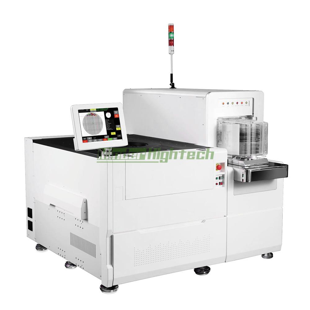
Product Introduction
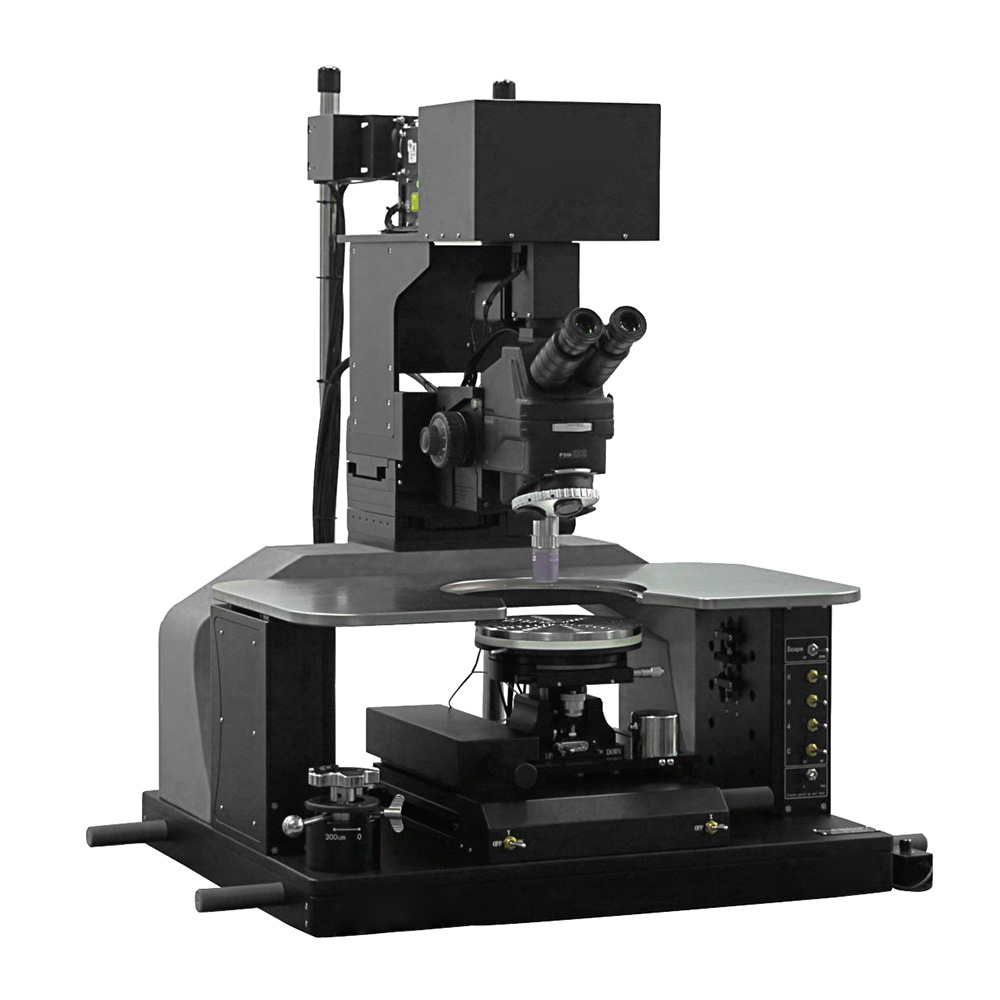
MDSM-FA12 is a 12-inch (compatible with 8-inch) high-per-formance wafer test probe station that completes the WAT/CP test through precise contact between probe cards and wafer PAD points.
The device is easy-to-use and has superior mechanical stability, which can provide customers with low-cost and high-yield wafer test solutions and meet the test requirements of different customers such as wafer manufacturers, chip package plants, test factories.
Product Features
1.High precision and test speed, greatly
improving test efficiency
2.Micron-level fully closed-loop motion
control
3.24*7 hours on-chip detection
4.Friendly user interface
5.Automatic wafer loading and unloading
6.High strength low center of gravity design
Product Parameters
|
Model |
MDSM-F12 |
|
|
Wafer |
Wafer diameter |
8inch,12inch |
|
Wafer thickness |
200-2000μm |
|
|
Die Size |
300-100000μm |
|
|
Weight |
≤500g |
|
|
Chuck |
XY Travel range |
X: ±170mm ; Y:-180,+600mm |
|
XY Repeatability |
≤±1µm |
|
|
XY Accuracy |
≤±2µm |
|
|
XY Resolution |
0.1µm |
|
|
XY Maximum speed |
240mm/s |
|
|
Z Travel range |
0-80mm |
|
|
Z Repeatability |
≤±1µm |
|
|
Z Accuracy |
≤±2µm |
|
|
Z Resolution |
0.1µm |
|
|
Z Maximum speed |
80mm/s |
|
|
Theta |
Theta Rotation Range |
±10° |
|
Theta Resolution |
0.00001° |
|
|
Cassette / Wafer Size |
6", 8", 12" |
|
|
Dimensions |
1595 x 1675 x 1500 mm |
|
|
Voltage |
50/60Hz AC220V |
|
|
CDA air pressure |
0.4-0.8MPA |
|
|
Vacuum pressure |
-70 to-90kpA |
|
联系人:胡顺语
手机:0086-15813334038
电话:020-84789496
邮箱:md@minder-hightech.com
地址: 广州市番禺区大龙街市新路新水坑段43号813