
Suitable for
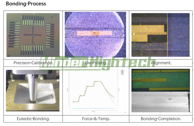
Providing ±0.5μm alignment accuracy, it is suitable for various precision positioning, chip placement, and various high-end packaging process applications, including flip-chip bonding, ultrasonic gold ball bonding, laser bar bonding, gold-tin eutectic bonding, and adhesive bonding.
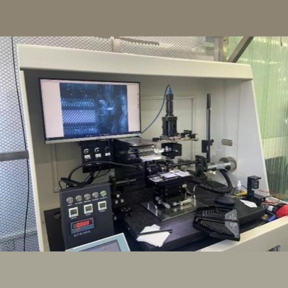
Introduction
1. Highly cost-effective equipment with a modular design and flexible configuration.
2. Suitable for various flip-chip, face-mounted chips, Micro LED applications, and covers nearly all micro-assembly and placement processes.
3. Primarily designed for small-batch production and to meet the needs of prototyping, R&D, and university teaching and research.
Features
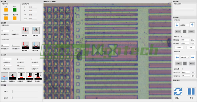
1.High-Precision Alignment.Relying on a fixed-position beam splitter alignment system, a high-resolution optical system, and a micron-level workbench, it achieves an alignment accuracy of ±0.5 µm, enabling precise control of operation details.
2. Automated Operation Software.The self-developed software integrates full-process operations to realize automation of die separation and bonding; it supports real-time viewing and storage of process curves, enabling efficient management and control of production processes.
3.Modular Design.Adopting a modular architecture, users can flexibly select and configure components (such as ultrasonic welding modules, formic acid modules) according to their needs, adapting to diverse production scenarios and improving equipment applicability.
4. Precise Control of Force and Temperature.The software has a built-in process recipe management interface, and real-time control of bonding force and temperature is achieved through algorithms, ensuring the stability of process parameters and facilitating high-quality production.
Processes
1.Thermal compression
2.Thermo-sonic(optional)
3.Ultrasonic(optional)
4.Reflowbonding(optional)
5.Dispensing (optional)
6.Mechanical assembly
7.UV curing(optional)
8.Eutecticbonding
Applications
1.Laser diode, laser bar bonding
2.VCSEL、PD、lens assembly packaging
3.Laser LED packaging
4.Laser through-hole packaging
5.MEMS/MOEMS packaging
6.Sensor packaging
7. 3D packaging
8.Wafer-level packaging (C2W)
9.Flip-chip bonding (face-down)
Technical Specifications
|
Model |
RYW-ETB05B |
RYW-ETB20 |
RYW-ETB05S |
RYW-ETB20S |
|
Alignment Accuracy |
±0.5μm |
±2μm |
±0.5μm |
±2μm |
|
Field of View |
0.5×0.3-5.4×4mm² |
1.2×0.9-14.4×10.8mm² |
0.5×0.3-5.4×4mm² |
1.2×0.9-14.4×10.8mm² |
|
Substrate Size |
150mm/6-inch(300mm/12-inch) |
|||
|
Chip Size |
0.1~40mm |
|||
|
Axis Fine Adjustment |
±10° |
|||
|
Fine Adjustment Range |
2.5×2.5×10mm Res(0.5μm) |
|||
|
Pressure Range |
0.2~30N(Option 100N) |
|||
|
Heating Temperature |
350±1℃ (Option 450℃) |
|||
|
Heating and Cooling Rates |
Heat: 1~100℃/s; Cool: >5℃/s |
|||
|
Operating Range |
100mm×200mm |
|||
|
Device Dimensions |
L0.7×W0.6×H0.5m |
|||
|
Operation Type |
Semi-Automatic Rotary |
Manual Rotary |
||
|
Device Weight |
120Kg |
100Kg |
||
联系人:胡顺语
手机:0086-15813334038
电话:020-84789496
邮箱:md@minder-hightech.com
地址: 广州市番禺区大龙街市新路新水坑段43号813