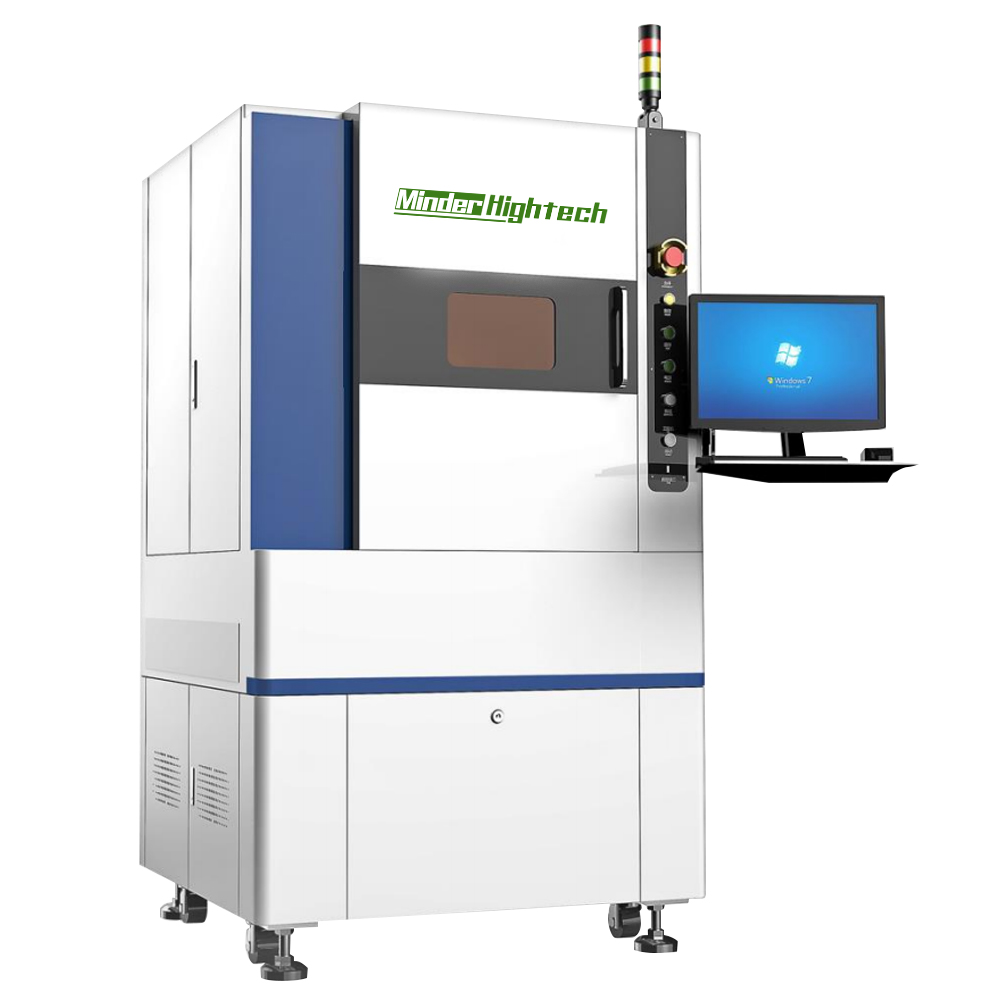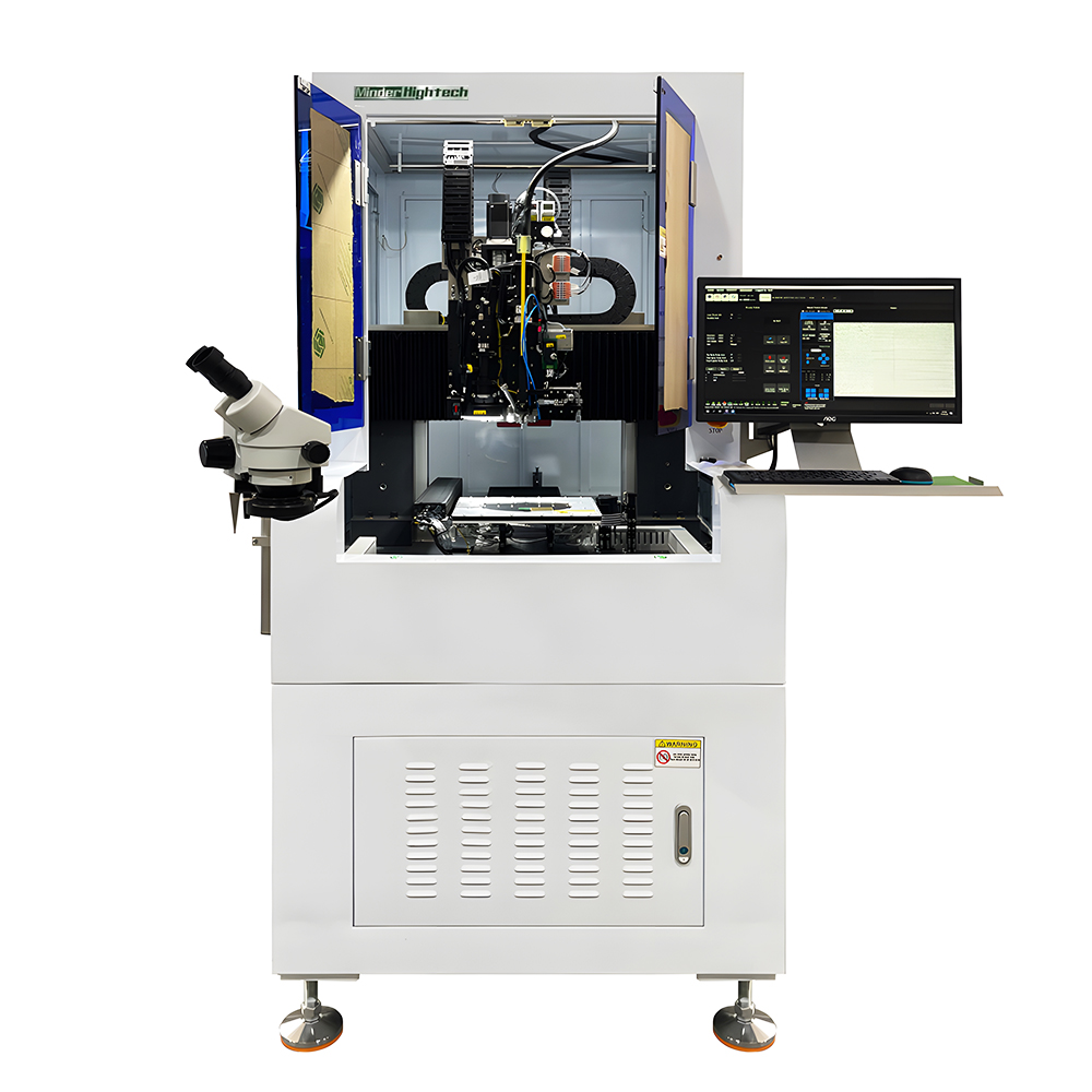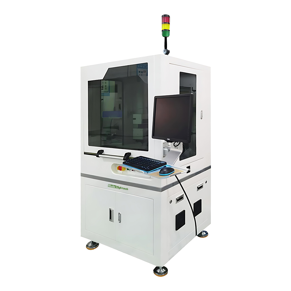

Wafer Stealth Laser Dicing system
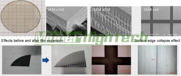
Wafer Stealth Laser Dicing, as a solution for laser dicing wafers, effectively avoids the problems of grinding wheel slicing. Laser Stealth dicing is achieved by shaping a single pulse of pulsed laser through optical means, allowing it to pass through the surface of the material and focus inside the material. In the focal area, the energy density is high, forming a multi photon absorption nonlinear absorption effect, which modifies the material to form cracks. Each laser pulse acts equidistant, forming equidistant damage to form a modified layer inside the material. At the position of the modified layer, the molecular bonds of the material are broken, and the connections of the material become fragile and easy to separate. After dicing, the product is fully separated by stretching the carrier film, creating gaps between the chips. This processing method avoids damage caused by direct mechanical contact and rinsing with pure water. At present, laser Stealth dicing technology can be applied to sapphire/glass/silicon and various compound semiconductor wafers.
Application:
The fully automatic wafer laser stealth dicing equipment is mainly suitable for various semiconductor materials such as silicon, germanium, silicon carbide, zinc oxide, etc. Stealth dicing is a dicing method that focuses laser light inside the workpiece to form a modified layer, and divides the workpiece into chips by expanding the adhesive film and other methods. It is suitable for 4-inch, 6-inch, and 8-inch&12inch wafers.
Dicing Samples
|
Processing size |
12 inches, 8 inches, 6 inches, 4 inches |
|
Processing method |
Cut/back cut |
|
Processing material |
Sa pphire、Si、GaN and other brittle materials |
|
Wafer thickness |
100-1000um |
|
Maximum processing speed |
1000/s |
|
Positioning accuracy |
1um |
|
Repeat positioning accuracy |
1um |
|
Edge collapse |
< 5um |
|
Weight |
2800kg |
|
NO. |
Project name |
Indicators |
|
1 |
Laser type |
Infrared laser (wavelength 1342nm) |
|
2 |
Laser power |
≥5W |
|
3 |
Beam spot elliptic ity |
≤85% |
|
4 |
Beam quality factor M2 |
≤ 1.3 |
|
5 |
X axis |
Stroke: ≥ 500mm, accuracy: ± 1um |
|
6 |
Y axis |
Stroke: ≥ 600mm, accuracy: ± 1um |
|
7 |
Z axis |
Stroke: ≥ 10mm, accuracy: ± 1um |
|
8 |
θ axis |
Stroke: ≥360° , rotation axis resolution: ≤0.0002° |
|
9 |
Stage size |
12 inches and backward compatible |
|
10 |
Cutting thickness |
Cutting thickness range needs to cover: 50um-1mm |
|
11 |
Loading and unloading method |
Fully automatic and manual compatible loading and unloading |
|
12 |
Scribing method |
Cut and back cut, modify the wafer by focusing the laser into the inside of the substrate (invisible cutting) |
|
13 |
Cutting axis speed |
0-1000mm/s |
|
14 |
Laser cutting line width |
≤2um |
|
15 |
Cutting edge collapse |
≤5um |
|
16 |
Cutting object |
SI/SIC silicon carbide wafer (wafer cutting path is free of foreign matter and dirt) |
|
17 |
Focus method |
Autofocus |
|
18 |
Focus accuracy |
± 1um |
|
19 |
Lighting system |
LED light source, adjustable brightness |
|
20 |
Processing end power measurement |
With processing end power measurement function |
联系人:胡顺语
手机:0086-15813334038
电话:020-84789496
邮箱:md@minder-hightech.com
地址: 广州市番禺区大龙街市新路新水坑段43号813